In a failed attempt to recover a bricked WDR4900 by serial, the bootloader in the flash memory was erroneously deleted or damaged. This makes things worse as without the device even booting, there is no more option to establish an emergency connection by serial cable.
In this post, a procedure is demonstrated which allows to recover the router by unsoldering the router’s memory chip and flashing it with an external SPI programming device.
Symptoms
When powering up the router, the LEDs on the front panel will behave as follows:
[table id=3 /]
Additionally of course, the router cannot neither be contacted by telnet, nor by ssh or serial cable.
Remedies
The only way to blow life back into the router is by one of those two methods.
- by JTAG or
- by unsoldering the flash chip and reflash it with an external device
I first tried to go for the JTAG solution as it would have spared me to desolder the chip from the router. Unfortunately, it was impossible to establish any communication between the FlashcatUSB and the JTAG interface. This might be due to the fact that the router board has a RISCWATCH/COP layout which probably differs from the EJTAG standard. The following procedure therefore only refers to directly flashing the SPI chip without passing through the JTAG interface.
Examination of the router
You can easily open the router as described in the first minutes of this video. Remove the 3 external antennas, unscrew the 4 screws at the bottom of the case and gently prey the plastic clips open which retain the cover of the plastic case. It is not necessary or advisable to take the board out, as this would require to unsolder the wires of the internal antennas. All work can be done with the router’s PCB remaining in the bottom part of the case and just the lid being removed.
The board
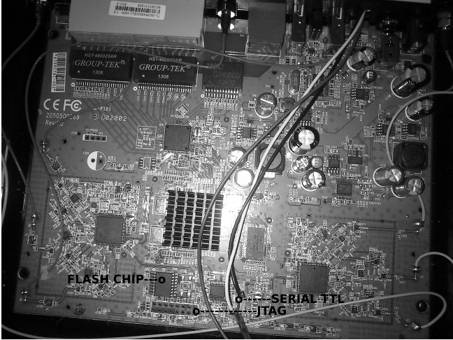
The image below shows the opened router with the flash chip. Note that the 3 DuPont cables in the photo have been added to provide an access to the serial TTL adapter without opening the case (the adapter is of no help though, as it can only be used when U-boot is working correctly).
Specs of the flash memory chip
As shown in the overview picture, the memory which holds the damaged bootloader and has to be flashed resides right above the JTAG port on the router board. According to the OpenWRT documentation for the WDR4900 it is a Spansion FL128SAIF00 chip (NOR type).
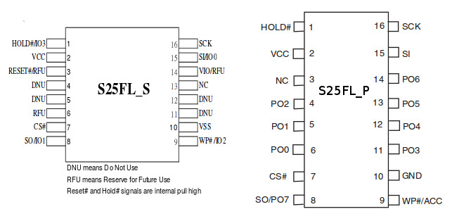
Pin-out
For starters, a good thing to know would be the pin-out on the Spansion memory chip. I found a Macronix document comparing the FL128S Spansion chip with the Macronix MX25L12835F chip which also shows the connection diagramm for our Spansion chip. Nothing surprising here, as the pin-outs for both the current S25FL128S and its P-series predecessor follow the standard layout for SPI chips.
Flash memory layout
Another piece of information we are going to need is the memory flash layout. Inside the u-boot environment of a working router, this can be retrieved with the help of the printenv command.
An alternative way to get the memory mapping is to check on a running router:
|
1 2 3 4 5 6 7 8 9 10 11 12 13 14 15 16 17 18 19 20 21 22 23 24 25 26 |
root@wdr4900:~# cat /proc/mtd dev: size erasesize name mtd0: 00050000 00010000 "u-boot" mtd1: 00010000 00010000 "dtb" mtd2: 002a0000 00010000 "kernel" mtd3: 00ce0000 00010000 "rootfs" mtd4: 002f0000 00010000 "rootfs_data" mtd5: 00010000 00010000 "config" mtd6: 00010000 00010000 "caldata" mtd7: 00f80000 00010000 "firmware" root@wdr4900:~# dmesg | grep u-boot [ 0.639973] 0x000000000000-0x000000050000 : "u-boot" root@wdr4900:~# dmesg | grep dtb [ 0.645617] 0x000000050000-0x000000060000 : "dtb" root@wdr4900:~# dmesg | grep kernel [ 0.650943] 0x000000060000-0x000000300000 : "kernel" root@wdr4900:~# dmesg | grep rootfs [ 0.656530] 0x000000300000-0x000000fe0000 : "rootfs" root@wdr4900:~# dmesg | grep rootfs_data [ 0.676082] 0x000000cf0000-0x000000fe0000 : "rootfs_data" root@wdr4900:~# dmesg | grep config [ 0.682077] 0x000000fe0000-0x000000ff0000 : "config" root@wdr4900:~# dmesg | grep caldata [ 0.687660] 0x000000ff0000-0x000001000000 : "caldata" root@wdr4900:~# dmesg | grep firmware [ 0.693322] 0x000000060000-0x000000fe0000 : "firmware" |
Summing up, we can assume that the flash memory layout is as follows:
[table id=6 /]
Data to be flashed
Now is a good moment to think about how to get hold of the data we want to flash. The first thing that comes to mind is to just download the original firmware from TP-Link’s home page or get hold of an OpenWRT image for that router.
Unfortunately, that won’t solve your problem because you just get mtd7 (or even less). What you need, though, is an image of the complete content of the flash memory inside the router. Sometimes, there are folks who upload these images to dev forums (e.g. there is someone who has uploaded the config partition (mtd5) here), so google around a bit. At this point I can only issue an urgent public service announcement by quoting Michael Kuron’s blog:
Why do people keep on ignoring all recommendations to MAKE A BACKUP OF YOUR ART PARTITION?
Dear Michael: The problem is probably not that people deliberately ignore your advice but rather that most people (myself unfortunately included) only read that advice when they have already damaged their mtd partitions. But I will do my very best to spread your recommendation.
So please – with extra sugar on top – if anyone reads this post before they have damaged their config and caldata partitions: Back up your mtd partitions before it’s too late! Even if you find someone who has got the exact same router model and version and who is kind enough to share his mtd partitions, there is a debate on whether the ART calibration data is so router specific, that your WLAN functionalities will later be buggy with an mtd5 partition copied from another device.
As I had a working twin router at home, I could dump the mtd images from that device. To dump a partition, just issue the following command on a working router’s console. As always when working with the dd command, be careful not to mix up anything – there is a reason why dd is nicknamed “disk destroyer”…
|
1 2 3 4 |
root@wdr4900:~# dd if=/dev/mtd0 of=/tmp/dev0_uboot.bin 640+0 records in 640+0 records out root@wdr4900:~# |
Proceed the same way for mtd1, mtd5, mtd6 and mtd7. mtd2 to mtd4 do not have to be dumped separately, as the firmware partition mtd7 includes these 3 partitions already. Once everything is dumped, transfer these files to your computer for further editing.
Editing the data
Before writing these dumps back into the memory chip, we should make sure that the MAC addresses coded into the dumps are in line with the MAC address printed on the bottom of our router’s case. We therefore open the mtd5 backup file with a hex editor and proceed as follows:
- With 0x0 being the initial address of the dump of
mtd5, we find the MAC address printed on the router label at offset 0x144. We will call this MAC address the “root MAC”. Set this root address to the values printed on your router’s label. - After two empty bytes at offsets 0x14a and 0x14b, there is a sequence of eight MAC addresses starting from offset 0x14c and ending at offset 0x17b. Each of these MAC addresses is generated by increasing the previous MAC address by one. If the root MAC address was 00:11:22:33:44:55, the first address in the sequence will be 00:11:22:33:44:56, the next 00:11:22:33:44:55:57 and the final (eighth) one will be 00:11:22:33:44:5d. Edit this sequence so that it matches the root MAC address you just set.
- The sequence of the eight MAC addresses derived from the “root address” is repeated starting at offset 0x17c and ending at 0x1ab. Make sure you adapt these MAC values, too.
- Inside both sequences and between sequences, there are no empty bytes or spaces as separators (unless a MAC address itself contains FF, of course).
Concatenation of the dumps
All we need to do now is to glue the dumps together to a single binary file to be flashed. Fortunately, with Linux, we can just cat them into a single file:
|
1 |
ilek@i7:/media/ramdisk$ cat mtd0.bin mtd1.bin mtd7.bin mtd5.bin mtd6.bin > flashfile.bin |
Tools needed for the flash procedure
[table id=13 /]
Unsoldering the flash chip
Although there are some people who try to re-program flash chips “in situ” – i.e. leaving the chip on the board and connecting the FlashcatUSB to the pins soldered to the board, the advice is normally to first unsolder the chip from the board and then connect it directly to the Flashcat (see this post for a different TP-Link model from someone who successfully reflashed his chip).
The safest way to unsolder the chip is to use a hot air gun. From my experience, the following settings on the Atten 838D are fine to unsolder the chip:
- Air Flow: 2 1/2 (go for a low air flow to prevent neighbouring parts being unintentionally blown from the board)
- Temperature: 350°C
- Nozzle size: medium
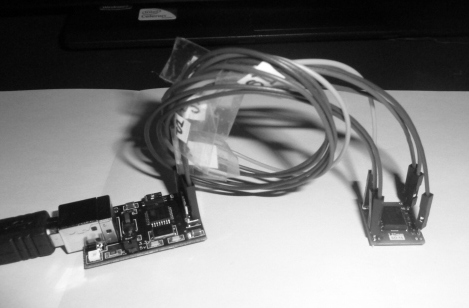
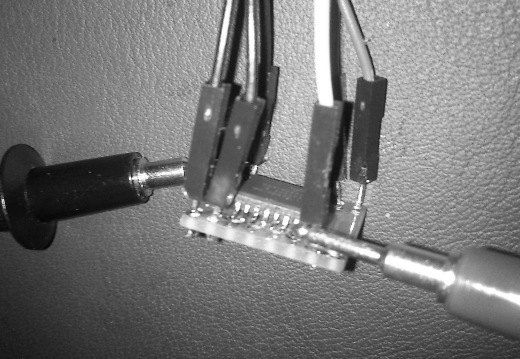
Connecting the chip
The next step is to solder the memory chip on a PCB testing board. Then solder the male ends of 6 DuPont cables to the appropriate points on the testing board and connect the female ends to the FlashcatUSB as shown in the diagram below.
Basic connection
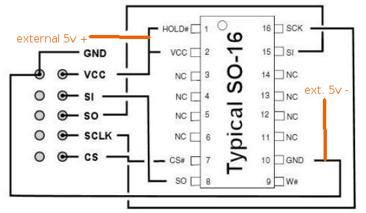
VCC and HOLD are both connected to the VCC cable to the FlashcatUSB. The easiest way to achieve this is to short circuit the soldering soldering points 1 and 2 on the testing PCB.
Power supply
The majority of failed attempts to flash the chip with the Flashcat are most probably due to insufficient power supply. For flashing the chip successfully it is essential to provide sufficient power – both in terms of tension and current. Symptoms for insufficently powered setups are:
- The Flashcat software fails to identify the chip. Or if the chip is correctly identified, one or more of the following problems pop up:
- Read operations produce spurious contents, i.e. if you read the contents of the same chip several times, you always get different results for the same content residing in the chip.
- Erase operations are finished in less than a second, but after the erase, the chip still contains data.
- Write operations fail with thousands of verify errors, and only a tiny fraction of data (if anything at all) is written to the chip. The software becomes unresponsive and after the write op is reported to be completed, the blue LED on the Flashcat keeps blinking for infinite time. The only way to get the Flashcat back into normal operation is to press its reset button.
5V power supply mandatory
Even though Spansion’s spec sheets for the memory chip suggest that the chip should be powered with 3.6V, flashing it with the Flashcat requires 5V.
You must therefore ensure that the power jumper on the Flashcat is set to 5V and not to 3.3V. Once again: The 3.3V setting will not work, but 5V will – and there is no reason to be afraid that your chip could be damaged by powering it with 5V.
External auxiliary power supply needed
One of the main problems with the power supply is that both the Flashcat and the memory chip get their power from a USB connector, which – according to the USB specifications – limits the current provided. This current is not high enough to supply sufficient power to the Flashcat and the chip while read and write operations are carried out.
It is therefore necessary to provide an auxiliary power supply with 5V constant voltage. The additions to the standard wiring according to the Flashcat documentation are shown in orange in the above connection diagram:
- The cable leading to pins 1 and 2 of the chip must be connected to both the Flashcat VCC pin and the VCC (+) of a 5V external power supply
- Likewise, the cable leading to pin 10 of the chip (GND) must be connected to both to the Flashcat GND pin and GND (-) of the 5V external power supply.
If you have some kind of cable with suitable crocodile clamps or similar, this would be an elegant way to connect the auxiliary power cables to the ends of the cables leading from the Flashcat to the PCB testing board with the chip. Me being an electronics amateur, I went the amateurish (or “dodgy”) way and took the two cables from my multimeter with one end plugged into my PSU and the probing ends held against the two pins during the flash procedure.
Flashing the firmware
If you have your flashfile ready and your chip connected, power up your FlashcatUSB under Windows, start the Flashcat software and write the file into the chip. I have made a short video of the flashing procedure here.
Note that the current display on the aux PSU jumps between 0 and 0.04A. This shows that the write operation needs about 40 mA more in current than what the computer’s USB port can deliver.
After the flash is done, it is advisable to read out the whole flash content once again and to make sure that there are no diffs against the flash file.
After successfully flashing desolder the chip from the testing PCB using the hot air gun. Flux the soldering pads on the router board, clean them a bit with the help of the solder wick, flux again and solder the chip back onto the board using the soldering iron. Make sure all pins are neatly soldered to the SMD pads of the board. Clean any flux remainders with isopropyl alcohol. The router can now be launched in normal operation as before.
Open Issues
There is one problem which has not yet been solved. If the twin router from which the mtds have been copied is operated at the same time as the recovered router, their WLANs seem to mix even though the MAC addresses and the SSID differ. It is therefore not possible to operate the WLANs of the donated router and the recovered router at the same time. I am going to investigate this problem and will come up with a solution as soon as I have sufficient information.